
Semiconductor package
This article needs additional citations for verification. (September 2011) |
A semiconductor package is a metal, plastic, glass, or ceramic casing containing one or more discrete semiconductor devices or integrated circuits. Individual components are fabricated on semiconductor wafers (commonly silicon) before being diced into die, tested, and packaged. The package provides a means for connecting it to the external environment, such as printed circuit board, via leads such as lands, balls, or pins; and protection against threats such as mechanical impact, chemical contamination, and light exposure. Additionally, it helps dissipate heat produced by the device, with or without the aid of a heat spreader. There are thousands of package types in use. Some are defined by international, national, or industry standards, while others are particular to an individual manufacturer.
Package functions[edit]
A semiconductor package may have as few as two leads or contacts for devices such as diodes, or in the case of advanced microprocessors, a package may have hundreds of connections. Very small packages may be supported only by their wire leads. Larger devices, intended for high-power applications, are installed in carefully designed heat sinks so that they can dissipate hundred or thousands of watts of waste heat.
In addition to providing connections to the semiconductor and handling waste heat, the semiconductor package must protect the "chip" from the environment, particularly the ingress of moisture. Stray particles or corrosion products inside the package may degrade performance of the device or cause failure.[1] A hermetic package allows essentially no gas exchange with the surroundings; such construction requires glass, ceramic or metal enclosures.

Date code[edit]
Manufacturers usually print the manufacturer's logo and the part number on the package using ink or laser marking. This makes it easier to distinguish the many different and incompatible devices packaged in relatively few kinds of packages. The markings often include a 4 digit date code, often represented as YYWW where YY is replaced by the last two digits of the calendar year and WW is replaced by the two-digit week number,[2][3] typically the ISO week number.
Very small packages often include a two-digit date code. One two-digit date code uses YW, where Y is the last digit of the year (0 to 9) and W starts at 1 at the beginning of the year and is incremented every 6 weeks (i.e., W is 1 to 9).[2] Another two-digit date code, the RKM production date code, use YM, where Y is one of 20 letters that repeat in a cycle every 20 years (for example, "M" was used to represent 1980, 2000, 2020, etc.) and M indicates the month of production (1 to 9 indicate January to September, O indicates October, N indicates November, D indicates December).
Leads[edit]
To make connections between an integrated circuit and the leads of the package, wire bonds are used, with fine wires connected from the package leads and bonded to conductive pads on the semiconductor die. At the outside of the package, wire leads may be soldered to a printed circuit board or used to secure the device to a tag strip. Modern surface mount devices eliminate most of the drilled holes through circuit boards, and have short metal leads or pads on the package that can be secured by oven-reflow soldering. Aerospace devices in flat packs may use flat metal leads secured to a circuit board by spot welding, though this type of construction is now uncommon.
Sockets[edit]
Early semiconductor devices were often inserted in sockets, like vacuum tubes. As devices improved, eventually sockets proved unnecessary for reliability, and devices were directly soldered to printed circuit boards. The package must handle the high temperature gradients of soldering without putting stress on the semiconductor die or its leads.
Sockets are still used for experimental, prototype, or educational applications, for testing of devices, for high-value chips such as microprocessors where replacement is still more economical than discarding the product, and for applications where the chip contains firmware or unique data that might be replaced or refreshed during the life of the product. Devices with hundreds of leads may be inserted in zero insertion force sockets, which are also used on test equipment or device programmers.
Package materials[edit]
Many devices are molded out of an epoxy plastic that provides adequate protection of the semiconductor devices, and mechanical strength to support the leads and handling of the package. The plastic can be cresol-novolaks, siloxane polyimide, polyxylylene, silicones, polyepoxides and bisbenzocyclo-butene.[4] Some devices, intended for high-reliability or aerospace or radiation environments, use ceramic packages, with metal lids that are brazed on after assembly, or a glass frit seal. All-metal packages are often used with high power (several watts or more) devices, since they conduct heat well and allow for easy assembly to a heat sink. Often the package forms one contact for the semiconductor device. Lead materials must be chosen with a thermal coefficient of expansion to match the package material. Glass may be used in the package as the package substrate to reduce its thermal expansion and increase its stiffness, which reduce warping and facilitate mounting of the package to a PCB.[5][6]
A very few early semiconductors were packed in miniature evacuated glass envelopes, like flashlight bulbs; such expensive packaging was made obsolete when surface passivation and improved manufacturing techniques were available.[1] Glass packages are still commonly used with diodes, and glass seals are used in metal transistor packages.
Package materials for high-density dynamic memory must be selected for low background radiation; a single alpha particle emitted by package material can cause a single event upset and transient memory errors (soft errors).
Spaceflight and military applications traditionally used hermetically packaged microcircuits (HPMs). However, most modern integrated circuits are only available as plastic encapsulated microcircuits (PEMs). Proper fabrication practices using properly qualified PEMs can be used for spaceflight.[7]
Hybrid integrated circuits[edit]

Multiple semiconductor dies and discrete components can be assembled on a ceramic substrate and interconnected with wire bonds. The substrate bears leads for connection to an external circuit, and the whole is covered with a welded or frit cover. Such devices are used when requirements exceed the performance (heat dissipation, noise, voltage rating, leakage current, or other properties) available in a single-die integrated circuit, or for mixing analog and digital functions in the same package. Such packages are relatively expensive to manufacture, but provide most of the other benefits of integrated circuits.
A modern example of multi-chip integrated circuit packages would be certain models of microprocessor, which may include separate dies for such things as cache memory within the same package. In a technique called flip chip, digital integrated circuit dies are inverted and soldered to a module carrier, for assembly into large systems.[8] The technique was applied by IBM in their System/360 computers.[9]
Special packages[edit]
Semiconductor packages may include special features. Light-emitting or light-sensing devices must have a transparent window in the package; other devices such as transistors may be disturbed by stray light and require an opaque package.[1] An ultraviolet erasable programmable read-only memory device needs a quartz window to allow ultraviolet light to enter and erase the memory. Pressure-sensing integrated circuits require a port on the package that can be connected to a gas or liquid pressure source.
Packages for microwave frequency devices are arranged to have minimal parasitic inductance and capacitance in their leads. Very-high-impedance devices with ultralow leakage current require packages that do not allow stray current to flow, and may also have guard rings around input terminals. Special isolation amplifier devices include high-voltage insulating barriers between input and output, allowing connection to circuits energized at 1 kV or more.
The very first point-contact transistors used metal cartridge-style packages with an opening that allowed adjustment of the whisker used to make contact with the germanium crystal; such devices were common for only a brief time since more reliable, less labor-intensive types were developed.[1]
Standards[edit]
Just like vacuum tubes, semiconductor packages standards may be defined by national or international industry associations such as JEDEC, Pro Electron, or EIAJ, or may be proprietary to a single manufacturer.
-
 Assorted discrete through-hole components
 -
 A microprocessor in a ceramic, dual in-line package with 48 pins.
 -
 A silicon wafer; individual devices (VLSI in squares) are not usable until diced, wire-bonded, and packaged
 -
 A plastic dual-in-line package containing an analog integrated circuit.This can be installed in a socket or directly soldered to a printed circuit board.
 -
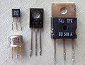
 A low current thyristor and a high power device, with a threaded stud for attachment to a heat sink, and a flexible lead; such packages are used for devices rated for hundreds of amperes.


See also[edit]
- Chip carrier
- Advanced packaging (semiconductors)
- Gold-aluminium intermetallic (purple plague)
- Integrated circuit packaging
- List of integrated circuit package dimensions
- IBM Solid Logic Technology
- Surface-mount technology
- Through-hole technology
References[edit]
- ^ a b c d Lloyd P.Hunter (ed.), Handbook of Semiconductor Electronics, McGraw Hill, 1956, Library of Congress catalog 56-6869, no ISBN chapter 9
- ^ a b "Quality & Lead-free (Pb-free): Marking Convention". Texas Instruments. Archived from the original on 2015-10-04. Retrieved August 6, 2015.
- ^ Vintage Calculators Web Museum: Frequently Asked Questions: "Date codes on electronics components and circuit boards". Retrieved 2020-04-23.
- ^ "Encapsulant - an overview | ScienceDirect Topics".
- ^ https://www.eetimes.com/intel-bets-on-glass-for-chip-substrate/
- ^ Delmdahl, Ralph & Paetzel, Rainer. (2014). Laser Drilling of High-Density Through Glass Vias (TGVs) for 2.5D and 3D Packaging. Journal of the Microelectronics and Packaging Society. 21. 53-57. 10.6117/kmeps.2014.21.2.053.
- ^ Ronald K. Burek, Johns Hopkins APL Technical Digest. “The NEAR Solid-State Data Recorders.” 1998. Retrieved August 6, 2015.
- ^ Keyan Bennaceur, Nature.com. “Mechanical Flip-Chip for Ultra-High Electron Mobility Devices.” September 22, 2015. April 23, 2015.
- ^ Michael Pecht (ed) Integrated circuit, hybrid, and multichip module package design guidelines: a focus on reliability, Wiley-IEEE, 1994 ISBN 0-471-59446-6, page 183