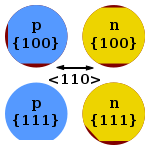
File:Wafer flats convention v2.svg

Size of this PNG preview of this SVG file: 150 × 150 pixels. Other resolutions: 240 × 240 pixels | 480 × 480 pixels | 768 × 768 pixels | 1,024 × 1,024 pixels | 2,048 × 2,048 pixels.
Original file (SVG file, nominally 150 × 150 pixels, file size: 13 KB)
File history
Click on a date/time to view the file as it appeared at that time.
| Date/Time | Thumbnail | Dimensions | User | Comment | |
|---|---|---|---|---|---|
| current | 21:40, 24 September 2013 |  | 150 × 150 (13 KB) | Cepheiden | fixed position of secondary flat Silicon processing for the VLSI era - Vol. 1 - Process technology; S Wolf; RN Tauber - Lattice Press; 1986; ISBN 096167237; p. 23 |
| 00:37, 23 December 2008 |  | 150 × 150 (13 KB) | Inductiveload | Added arrow indication <110> direction and enlarged flats so they can be easily seen | |
| 21:17, 29 February 2008 |  | 150 × 150 (9 KB) | Twisp | ||
| 21:13, 29 February 2008 |  | 150 × 150 (9 KB) | Twisp | ||
| 21:06, 29 February 2008 |  | 150 × 150 (8 KB) | Twisp | ||
| 20:59, 29 February 2008 |  | 150 × 150 (8 KB) | Twisp | ||
| 18:09, 29 February 2008 |  | 150 × 150 (9 KB) | Twisp | {{Information |Description= Wafer flats convention, based on Image:Wafer flats convention.PNG Conventional meaning of ''flats'' in semiconductor wafers. Black denotes material that has been removed. Wafer orientation is |
File usage
The following pages on the English Wikipedia use this file (pages on other projects are not listed):
Global file usage
The following other wikis use this file:
- Usage on ca.wikipedia.org
- Usage on cs.wikipedia.org
- Usage on de.wikipedia.org
- Usage on es.wikipedia.org
- Usage on et.wikipedia.org
- Usage on eu.wikipedia.org
- Usage on fi.wikipedia.org
- Usage on it.wikipedia.org
- Usage on it.wikibooks.org
- Usage on ja.wikipedia.org
- Usage on ko.wikipedia.org
- Usage on nl.wikipedia.org
- Usage on pl.wikipedia.org
- Usage on ro.wikipedia.org
- Usage on sk.wikipedia.org
- Usage on uk.wikipedia.org
- Usage on www.wikidata.org
